


.jpg)
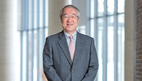
三澤 明
| 所属 | 情報システム工学科 |
|---|---|
| 職名・学位 | 教授・博士(工学) |
| 研究室 | H209 |
学部担当科目
センサネットワーク、情報システム工学演習、線形代数学Ⅱ、情報通信ネットワーク工学、ハードウェアデザインプロジェクト、電子回路実習
大学院担当科目
<博士前期課程>
技術経営特論
技術経営特論
経歴
| 昭和63年3月 | 北海道大学工学部電子工学科卒業 |
| 平成2年3月 | 北海道大学大学院工学研究科電子工学専攻修了 |
| 平成2年4月 | 日本電信電話株式会社 交換システム研究所 |
| 平成9年7月 | 日本電信電話株式会社 光ネットワーク研究所 |
| 平成11年1月 | 日本電信電話株式会社 第三部門R&Dビジョン担当 |
| 平成13年7月 | 日本電信電話株式会社 未来ネットワーク研究所 |
| 平成20年7月 | 西日本電信電話株式会社 研究開発センタ プロジェクトマネージャ |
| 平成22年7月 | 日本電信電話株式会社 NWサービスシステム研究所 グループリーダ |
| 平成28年3月 | 北海道大学大学院情報科学研究科メディアNW専攻博士後期課程修了 |
| 平成29年4月 | 千歳科学技術大学 情報システム工学科 教授 |
| 平成31年4月 | 公立千歳科学技術大学理工学部情報システム工学科 教授 |
専門分野
通信工学、情報通信システム(IPネットワーク、光スイッチングシステム)
現在の研究テーマ
センサーネットワーク、IoT通信方式
所属学会
IEEE Communication Society
電子情報通信学会(フォトニックネットワーク研究専門委員)
電子情報通信学会(フォトニックネットワーク研究専門委員)
主な著書及び解説
- “複数レイヤによるGMPLSシグナリング相互接続実験に成功―日本発の次世代光通信の世界標準確立に向け前進―”,電子情報通信学会誌2003年9月
- “次世代コアネットワークの高度制御技術―マルチレイヤ連携機能―“,NTT技術ジャーナル2003年9月
- “IPネットワークの信頼性について”,日本信頼性学会誌2011年1月
- “柔軟なサービス振り分けを実現するエッジルータシステム”,NTT技術ジャーナル2016年2月
論文
- K. Hayata, A. Misawa, and M. Koshiba, “Nonlinear Beam Propagation in Tapered Waveguides,” IEE Electron. Lett., vol. 25, no. 10, pp.661-662, May 1989.
- 早田和弥,三澤明,小柴正則,“複素誘電媒質からなる結合導波系の水平横モード解析―位相同期半導体アレーレーザへの応用―”,信学論Vol. J72-C1 No.11, pp.812-819 (1989.11)
- K. Hayata, A. Misawa, and M. Koshiba, “Nonstationary Simulation of Nonlinearly Coupled TE-TM Waves Propagating Down Dielectric Slab Structures by the Step-By-Step Finite-Element Method,” OSA Optics Letters, Vol. 15, Issue 1, pp. 24-26, Jan. 1990.
- 早田和弥,三澤明,小柴正則,“直接積分法を用いた非線形光導波系の有限要素シミュレーション”,信学論Vol. J73-C1 No.4, pp.151-157 (1990.4)
- K. Hayata, A. Misawa, and M. Koshiba, “Chaotic Propagation of the Elliptically-Polarized Light in Nonlinear Guided-Wave Structures,” Trans. of the IEICE, vol. E73, no. 6, pp. 855-860, June 1990.
- K. Hayata, A. Misawa, and M. Koshiba, “Spatial Polarization Instabilities due to Transverse Effects in Nonlinear Guided-Wave Systems,” J. Opt. Soc. Am. B, Vol. 7, Issue 7, pp. 1268-1280, July 1990.
- K. Hayata, A. Misawa, and M. Koshiba, “Split-step Finite-Element Method Applied to Nonlinear Integrated Optics,” J. Opt. Soc. Am. B, Vol. 7, Issue 9, pp. 1772-1784, Sep. 1990.
- A. Misawa, H. Nakano, and T. Matsunaga, “Signal Self-Thresholding using Wavelength-Division Multiplexed Differential Transmission for Photonic ATM Switches, “ IEE Electron Lett., vol. 29, no. 15, pp. 1337-1338, July 1993.
- M. Tsukada, A. Misawa, J. Nishikido, Y. Shimazu, H. Nakano, “Experiments on Photonic Cell Switching with an Optical Input Buffer,” IEE Electron Lett., vol. 30, no. 13, pp. 1081-1082, April 1994.
- A. Misawa, K. Sasayama, and T. Matsunaga, “Fast Wavelength Selection for Four-Channel Wavelength-Division-Multiplexed 10-Gbit/s Optical Cells,” IEE Electron Lett., vol. 31, no. 20, pp. 1762-1763, Sept. 1995.
- A. Misawa and T. Matsunaga, “Q factor Measurements of Photonic ATM Switch with Four-Channel FDM Output Buffer at 2.5 and 10 Gbit/s,” IEE Electron Lett., vol. 32, no. 17, pp. 1604-1605, April 1996.
- A. Misawa, Y. Yamada, M. Tsukada, K. Habara, and T. Matsunaga, “20 Gbit/s Photonic ATM Switching with Differential Packet Receiver, “ IEE Electron Lett., vol. 32, no. 19, pp. 1798-1799, Sep 1996.
- A. Misawa and T. Matsunaga, “Optical Input Buffers for the HiPower Photonic ATM Switch-Analysis and Experiments,” IEEE J. Lightwave Technol., vol. 14, no.10, pp. 2173-2183, Oct. 1996.
- Y. Yamada, K. Habara, A. Misawa, K. Sasayama, M. Tsukada, and T. Matsunaga, “Prototype of Frequency-Routing Type Photonic ATM Switch (FRONTIERNET) with Cascaded Optical Buffers,” IEE Electron Lett., vol. 33, no. 6, pp. 516-517, Mar. 1997.
- A. Misawa and M. Tsukada, “Broadcast-and-Select Photonic ATM Switch with Frequency Division Multiplexed Output Buffers,” IEEE J. Lightwave Technol., vol. 15, no.10, pp. 1769-1777, Oct. 1997.
- Y. Yamada, K. Sasayama, K. Habara, A. Misawa, M. Tsukada, T. Matsunaga, and K. Yukimatsu, “Optical Output Buffered ATM Switch Prototype Based on FRONTIERNET Architecture,” IEEE J. Select. Area on Commun., vol. 16, no. 7, pp. 1298-1308, Sep. 1998.
- A. Misawa, Y. Yamada, M. Tsukada, K. Sasayama, K. Habara, T. Matsunaga, and K. Yukimatsu, “A Prototype Broadcast-and-Select Photonic ATM Switch with a WDM Output Buffer,” IEEE J. Lightwave Technol., vol.16, no.12, pp.2202-2211, Dec. 1998.
- A. Misawa, K. Sasayama and Y. Yamada, “WDM Knockout Switch with Multi-Output-Port Wavelength-Channel Selectors,” IEEE J. Lightwave Technol., vol.16, no.12, pp.2212-2219, Dec. 1998.
- S. Mino, T. Matsunaga, Y. Shibata, A. Misawa, Y. Yamada, K. Habara, “Q-Factor-Based Level Design for Photonic ATM Switches,” IEICE Trans. Commun., vol. E82-B, No. 2, pp. 288-297, Feb. 1999.
- A. Misawa, K. Sasayama and T. Matsunaga, “Two-Output-Port Fast Tunable Filter with Low Loss and Low Loss Variation for 32 Wavelength Channels,” IEE Electron Lett., vol. 35, no. 8, pp. 657-658, April 1999.
- M. Nakagawa, K. Hattori, N. Kimishima, M. Katayama, and A. Misawa, “Hierarchical Time-Slot Allocation for Dynamic Bandwidth Control in Optical Layer-2 Switch Network,” IEICE Trans. Commun., vol. E97-B, No. 7, pp. 1303-1312, July 2014.
- M. Nakagawa, K. Hattori, N. Kimishima, M. Katayama, and A. Misawa, “Proposal of Rip-up & Re-allocate Algorithm for Optical Layer-2 Switch Network,” ATCA Photnica Sinica, vol. 43, No. 7, pp. 1-8, July 2014.
- K. Hattori, T. Homemoto, M. Nakagawa, N. Kimishima, M. Katayama, and A. Misawa, “Optical Layer-2 Switch Network with Bufferless Optical TDM and Dynamic Bandwidth Allocation”, IEICE Trans. Electron., vol.E99-C, No.2, pp.189-202, Feb. 2016.
- A. Misawa, K. Mochizuki, H. Tsuchiya, M. Nakagawa, K. Hattori, M. Katayama, and J. Kani, “Virtual Edge Architecture with Optical Bandwidth Resource Control,” IEICE Trans. Commun., vol. E99-B, No. 8, pp. 1805-1812, Aug. 2016.